17758013020 Chen Chen
-
-
-
17816169069 Jinglin Jian
-
17758013020 Chen Chen
17816169069 Jinglin Jian

Prof. Yang Xu is an IEEE NTC Distinguished Lecturer (2022 & 2023), Fellow of the Institute of Physics (FInstP), Fellow of the Royal Society of Chemistry (FRSC), Fellow of the Institute of Materials, Minerals and Mining (FIMMM), and IEEE EDS Senior Member. He is an editorial board member of IOP Nanotechnology and Associate Editor of IEEE T-ED, Photonics Research and Microelectronics Journal. He received his B.S. degree in Institute of Microelectronics at department of EE from Tsinghua University, M.S. and Ph.D. degrees in ECE from the University of Illinois Urbana-Champaign (UIUC), USA. He is a full professor and was served as Assistant Dean at the School of Micro-Nano Electronics, Zhejiang University, China. He was also a visiting-by-Fellow of Churchill College at the University of Cambridge, UK, and a visiting professor at the University of California Los Angles (UCLA). He has published more than 150 papers including Nature Electronics, Nature Nanotechnology, Nature Photonics, Chemical Reviews, and IEDM, etc. He authored one Wiley book titled as《Graphene for Post-Moore Silicon Optoelectronics》. He holds over 30 granted patents and gave more than 50 talks in international conferences. He also served as TPC of IEEE-EDTM and IEEE-IPFA conferences, and is technical committee member of IEEE EDS optoelectronic devices and IEEE NTC nanoelectronics (TC6). His current research interests include emerging 2D/3D integrated nano-devices and image sensors for Internet-of-Everything and Post-Moore Ubiquitous Electronics.
Multilayer Graphene/Silicon Broadband Photodetectors
Xiaoxue Cao1, 2, Chao Gao2, and Yang Xu1,2*
1 School of Micro-Nano Electronics, ZJU-Hangzhou Global Scientific and Technological Innovation Center, State Key Laboratory of Silicon and Advanced Semiconductor Materials, ZJU-UIUC Joint Institute, Zhejiang University, Hangzhou 310027, China
(Email: yangxu-isee@zju.edu.cn;xiaoxue_cao@zju.edu.cn)
2 MOE Key Laboratory of Macromolecular Synthesis and Functionalization, Department of Polymer Science and Engineering, International Research Center for X Polymers, Zhejiang University, Hangzhou 310027, China (chaogao@zju.edu.cn)
Abstract
Broad-spectrum detection and large-scale integration are the inevitable trends in the current evolution of infrared photodetectors. New materials were integrated with existing platforms to further improve the performance of infrared photodetectors. We reported a defective macro-assembled graphene nanofilm (D-nMAG)/Silicon (Si) photodetector using trap-assisted gain to optimize the photoelectric response. This waferscale environmentally friendly carbon material can be easily compatible with the complementary-metal-oxidesemiconductor (CMOS) technical as shown in Figure 1a-b. Noteworthy, the defective states in D-nMAG trap carriers and then enter the conduction and valence band again to be thermalized, generating a gain in photocurrent. Thus, our DnMAG-based line array image sensor exhibits high-resolution infrared imaging of the target as shown in Figure 1b-d. This device displays a high responsivity at room temperature within a broad-spectrum region, i.e., 0.156 A/W @ 900 nm in the nearinfrared (NIR) region and 3.7 mA/W @ 4 μm in the mid-infrared (MIR) region.
Additionally, we proposed a sputtering-lithography-annealing (SLA) strategy for patterning graphene nanofilm with pattern sizes ranging from microns to 100 nm scale without lattice damage as shown in Figure 2a-b. The sputtered masking agents can introduce easily repairable defects into graphene films compared the conventional patterning strategies. Especially, defects introduced by aluminum can be removed entirely. Based on the benefits of the bulk phase effect of nMAG, nMAG-based infrared detectors have significant prospective applications in infrared detection (Figure 2c). The carrier mobilities of intrinsic, sputtering, and repairing nMAG are 1530, 1410, and 1524 cm2 V-1 s-1, respectively. Compared with intrinsic nMAG, the carrier mobility of nMAG shows a 7.8% reduction after sputtering and a recovery to 99.6% after thermal treatment. These results confirm the advantages of the SLA strategy in patterning 2D materials.To further confirm the validity of the SLA strategy, we prepared macro-assembled graphene nanofilms (nMAG)/Ge and nMAG/Si heterojunction arrays for infrared detection as shown in Figure 2d. The patterned detectors present a responsivity of 0.09 A/W at 2 μm (nMAG/Ge) and 26.4 mA/W at 1550 nm (nMAG/Si) with a high array homogeneity as shown in Figure 2e-f, similar to the devices without patterning. This strategy lays the foundation for further exploration of new superstructures of nMAG and can be extended to other 2D materials. And our work provides a carbon nanofilm for IR detection at a broad-spectrum region, with tunable defective structure, uniform thickness, and wafer-scale production.
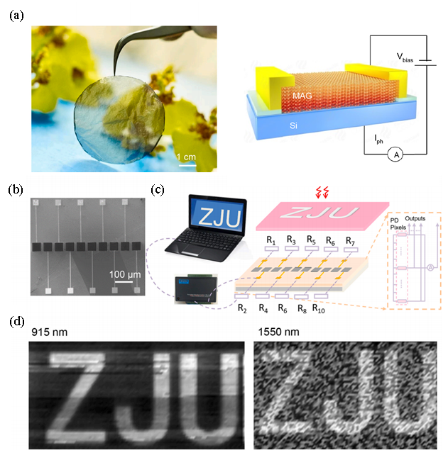
Figure 1: D-nMAG/ Si photodetector. (a) The photo of the D-nMAG/Si wafer (2-inches) and schematic of D-nMAG/Si device. (b) The SEM image of the D-nMAG/Si line array device. (c) The imaging schematic of the line array device. (d) The photograph of “ZJU” imaged by line array devices at 915 nm and 1550 nm wavelength with 2 mW/mm2 power density, respectively.
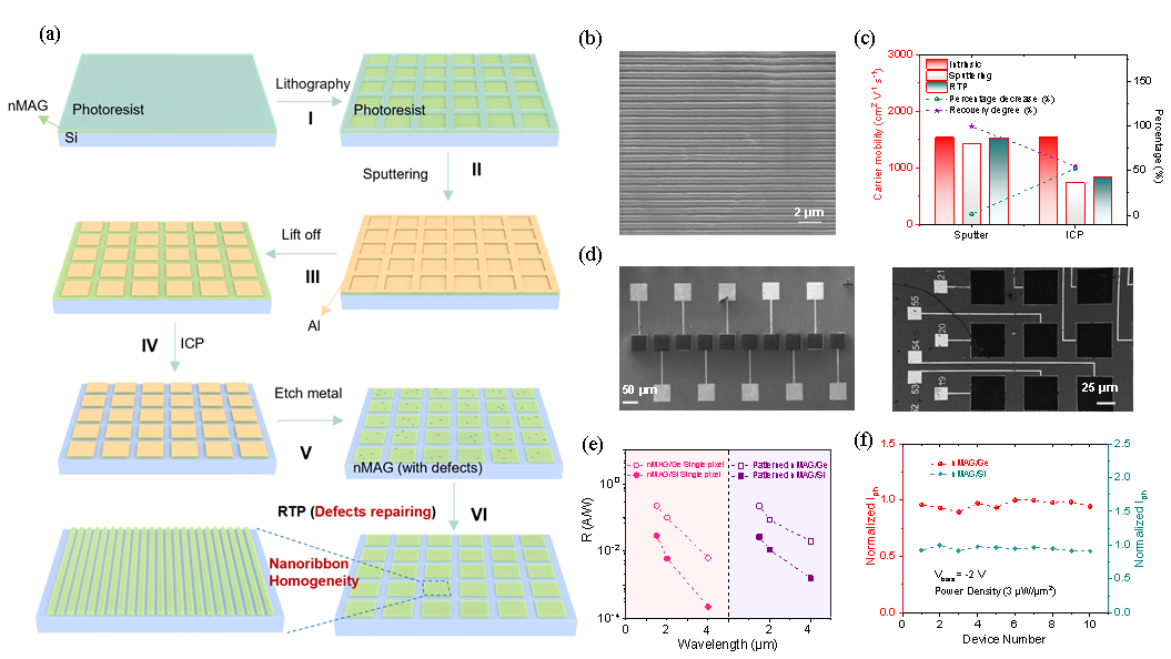
Figure 2: Graphene infrared photodetectors based on SLA strategy. (a) The schematic of recoverable patterned-nMAG. (b) SEM images of patterned-nMAG (feature Size: 100 nm). (c) The carrier mobility of nMAG. (d) The SEM image of the nMAG/Ge (Si). (e) The responsivity of nMAG/Si and nMAG/Ge as a function of wavelength. (f) Uniformity of line array devices under laser illumination at 1550 nm wavelength with 3 μW/μm2 power density.